Through-Hole vs SMD Soldering: Which to Learn First and How
The world of electronics is a fascinating realm of blinking lights, intricate circuits, and endless possibilities. Whether you’re dreaming of building your own custom gadgets, repairing beloved electronics, or diving deep into the world of microcontrollers and automation, soldering is an indispensable skill you’ll need to master. But as you embark on this journey, you’ll quickly encounter two primary methods of attaching components to a circuit board: Through-Hole Technology (THT) and Surface-Mount Technology (SMT).
These two approaches represent distinct eras and philosophies in electronics manufacturing, each with its own set of challenges, advantages, and required techniques. For the aspiring hobbyist or professional, understanding both, and more importantly, knowing where to begin, is crucial. This guide will walk you through the fundamental differences, explain why a particular starting point is recommended, detail the step-by-step techniques, outline the essential gear, suggest a practical learning path, highlight common pitfalls, and answer some frequently asked questions to set you firmly on the path to soldering mastery.
The Two Worlds: Through-Hole vs. Surface-Mount
Before we dive into the ‘how-to,’ let’s establish a clear understanding of what defines these two fundamental approaches to populating a Printed Circuit Board (PCB).
Through-Hole Technology (THT)
Through-Hole components are the veterans of the electronics world, the method that dominated circuit board assembly for decades. As the name suggests, these components feature wire leads that are inserted through drilled holes in the PCB. Once inserted, the leads are typically bent slightly on the underside of the board to hold the component in place, and then soldered to the copper pads surrounding the holes.
Key characteristics of Through-Hole components and soldering:
- Physical Size: Generally larger than their surface-mount counterparts, making them easier to handle and visually inspect.
- Mechanical Strength: The leads passing through the board provide a very strong mechanical connection, making through-hole components highly resistant to physical stress, vibration, and impact. This is why you often find them in applications where robustness is critical, such as power supplies, connectors, and heavy-duty switches.
- Ease of Soldering: The larger pads and leads offer a more forgiving target for a soldering iron, making the process less precise and more tolerant of minor errors in hand-eye coordination.
- Desoldering and Rework: Removing and replacing through-hole components is generally straightforward with basic tools like a solder sucker or wick, as the larger leads and pads are more resilient to repeated heating cycles.
- Heat Dissipation: Larger packages often have better inherent heat dissipation capabilities.
- Dominance: While still prevalent in certain applications, through-hole has largely been superseded by surface-mount technology in high-volume, compact electronics.
Surface-Mount Technology (SMT)
Surface-Mount Technology, often referred to by its components as Surface-Mount Devices (SMD), represents the modern standard in electronics manufacturing. Instead of leads passing through holes, SMD components are designed to be mounted directly onto the surface of the PCB. They have small metal contacts (pads or leads) on their underside or sides that make electrical contact with corresponding pads on the PCB surface.
Key characteristics of Surface-Mount components and soldering:
- Physical Size: Significantly smaller, sometimes microscopically so, allowing for much higher component density on a PCB. This miniaturization is critical for compact modern devices like smartphones, smartwatches, and highly integrated IoT sensors.
- Space Efficiency: No holes are drilled through the board, freeing up valuable PCB real estate and allowing components to be mounted on both sides of the board.
- Electrical Performance: The shorter leads and smaller parasitic capacitances/inductances of SMD components can lead to improved high-frequency performance and reduced noise.
- Manufacturing Efficiency: SMT is highly automated, utilizing pick-and-place machines for rapid and precise assembly, which is incredibly efficient for mass production.
- Challenges for Manual Soldering: The small size and tight pin pitches of many SMD components make manual soldering considerably more challenging, requiring finer tools, magnification, and more refined techniques.
- Heat Sensitivity: Smaller components can be more susceptible to overheating during manual soldering if not handled carefully.
- Dominance: SMT is the undisputed king of modern electronics manufacturing, found in virtually every consumer electronic device produced today, from the smallest sensors to complex computer motherboards.
In essence, through-hole is robust and beginner-friendly, while surface-mount is compact, high-performance, and dominant in contemporary electronics, though more demanding to work with manually.
Why Beginners Should Start Through-Hole
Given the ubiquity of SMD in modern electronics, you might be tempted to jump straight into learning surface-mount soldering. However, for almost every beginner, starting with through-hole technology is not just recommended, it’s essential for building a strong foundation. Here’s why:
- Larger Targets, Greater Forgiveness: Through-hole components are significantly larger. Their leads and the copper pads on the PCB are easier to see, easier to align, and present a much larger target for your soldering iron tip. This means you have more room for error as you develop your hand-eye coordination and learn to control the iron. Mistakes are less catastrophic and easier to correct.
- Fundamental Principles Made Clear: Through-hole soldering provides a clearer demonstration of the core principles of good soldering:
- Heat Transfer: You can visually observe the heat flowing from the iron tip to both the component lead and the PCB pad, and then to the solder.
- Wetting: It’s easier to see the solder flow smoothly and “wet” both the lead and the pad, forming a strong, shiny connection rather than just sitting as a dull blob.
- Capillary Action: You can observe the solder being drawn into the joint by capillary action. This visual feedback is invaluable for understanding why certain techniques work and what a good solder joint should look like.
- Less Specialized Equipment Initially: To start through-hole soldering, you primarily need a good temperature-controlled soldering iron, some solder, and basic hand tools. While a fume extractor and desoldering tools are highly recommended, you don’t immediately need magnification, hot air stations, solder paste, or fine-tipped tweezers, which are often necessary for SMD work. This lowers the barrier to entry and allows you to invest in essential tools first.
- Develops Core Skills: The skills you hone with through-hole soldering—iron control, heat management, solder application, component placement, and joint inspection—are directly transferable to SMD. Once you’ve mastered these fundamentals on a larger scale, scaling down to SMD becomes an exercise in precision and adaptation, rather than learning everything from scratch.
- Easier Rework and Troubleshooting: When you inevitably make a mistake (and you will, everyone does!), through-hole joints are much easier to desolder and rework. This allows for more practice in correcting errors without damaging expensive components or PCBs, fostering a less frustrating learning environment. Troubleshooting circuits built with through-hole components is also often simpler due to their larger size and more accessible test points.
- Build Confidence and Patience: Successfully soldering through-hole components builds confidence and patience, two critical attributes for any electronics hobbyist. The immediate gratification of seeing a functional circuit you’ve assembled yourself is a powerful motivator to continue learning.
Think of through-hole soldering as the essential “driving school” before you tackle the “Formula 1 track” of SMD. It teaches you the rules of the road, how to steer, how to brake, and how to navigate, all in a forgiving environment. Once you’ve got that down, you can start learning the advanced maneuvers required for high-performance driving.
Through-Hole Technique Step-by-Step
Mastering through-hole soldering involves a series of precise steps designed to create a strong, reliable electrical and mechanical connection. Follow these guidelines for consistent success:
1. Preparation is Key
- Cleanliness: Ensure your workspace is clean, well-lit, and well-ventilated (a fume extractor is highly recommended). Make sure your PCB and component leads are clean and free of grease or oxidation.
- Soldering Iron: Use a temperature-controlled soldering iron. For most leaded solder, a temperature between 320°C (600°F) and 370°C (700°F) is a good starting point. Lead-free solder often requires higher temperatures, around 370°C (700°F) to 400°C (750°F).
- Clean and Tin the Tip: The tip of your soldering iron should always be clean and shiny (tinned) with a thin layer of solder. Use a damp sponge or brass wool cleaner to wipe off old solder and oxidation. Immediately apply a small amount of fresh solder to the clean tip. A well-tinned tip transfers heat efficiently.
- Select Solder: For beginners, rosin-core leaded solder (e.g., 60/40 tin/lead or 63/37 tin/lead) is easier to work with due to its lower melting point and better flow characteristics compared to lead-free solder. A thin gauge (0.6mm-1.0mm) is generally suitable.
2. Component Placement
- Insert Component: Carefully insert the component leads through the correct holes on the PCB. Pay attention to polarity for components like diodes, LEDs, electrolytic capacitors, and integrated circuits (ICs).
- Secure Component: On the underside of the board, gently bend the leads outwards (e.g., at a 45-degree angle) to hold the component firmly in place against the board. This prevents it from falling out while you’re soldering.
3. Heat the Joint, Not the Solder
This is perhaps the most critical principle in good soldering.
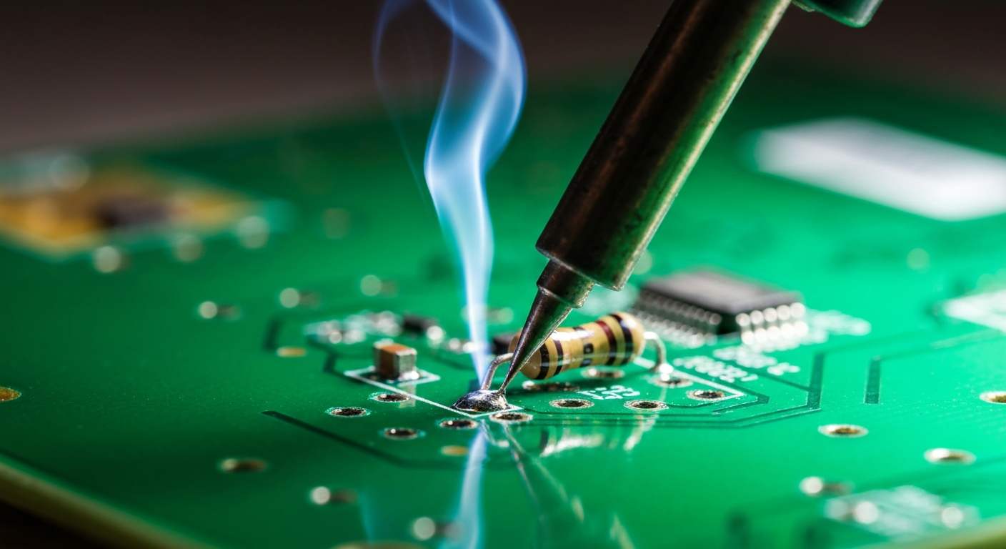
- Position the Iron: Bring the clean, tinned tip of your soldering iron into contact with both the component lead and the copper pad simultaneously. The goal is to heat both surfaces to the solder’s melting temperature at the same rate. The iron tip should make good contact with as much surface area of the lead and pad as possible.
4. The 1-2 Second Touch: Apply Solder
- Apply Solder Wire: After about 1-2 seconds of heating the joint, touch the solder wire to the opposite side of the joint from the iron tip. Do not touch the solder wire directly to the iron tip. The molten solder from the tip will help conduct heat, and the solder wire should melt and flow smoothly onto the heated lead and pad, not just blob onto the hot iron.
- Flow and Fill: Allow the solder to flow naturally around the lead and onto the pad, forming a smooth, concave fillet. Use just enough solder to cover the pad and form a good connection – don’t overdo it. The solder should be drawn into the joint by capillary action, indicating proper wetting. This usually takes another 1-3 seconds.
5. Remove Solder, Then Iron
- Remove Solder Wire: Once a sufficient amount of solder has flowed and the joint looks good, remove the solder wire from the joint.
- Remove Soldering Iron: Immediately after removing the solder wire, remove the soldering iron. Avoid holding the iron on the joint for too long, as this can overheat the component or lift the copper pad from the PCB. The entire heating and soldering process for one joint should ideally take no more than 3-5 seconds.
6. Inspect and Clip
- Cool Down: Allow the solder joint to cool naturally and solidify without disturbing it. Blowing on it is generally not recommended as it can lead to cold joints or dull finishes.
- Inspect the Joint: A good solder joint should be:
- Shiny and Smooth: Not dull, grainy, or lumpy.
- Concave (Volcano Shape): The solder should flow up the lead and onto the pad, forming a smooth, gentle slope, like a mini volcano. It should not be a convex blob.
- Wetted: The solder should clearly adhere to both the component lead and the PCB pad, indicating a strong electrical and mechanical bond.
- No Bridges: Ensure no solder has inadvertently connected to an adjacent pad or lead.
- Clip Leads: Once you’re satisfied with the joint, use flush cutters to trim the excess component lead as close to the solder joint as possible, without cutting into the joint itself.
Repeat this process for all leads of the component, and then for all other through-hole components on your board. For instance, learning to solder these components is a vital skill for projects like those found in our guide to /esp32-home-automation-projects/, where custom PCBs often feature a mix of component types.
SMD Technique
Once you’ve mastered through-hole, you’re ready to tackle the miniature world of SMD. SMD soldering requires more precision, specialized tools, and different techniques due to the tiny size of the components and the absence of through-holes. There are several primary methods for manual SMD soldering:
1. Iron Soldering (for larger SMDs)
This is the closest to through-hole technique and suitable for larger SMD resistors, capacitors (0805, 0603 sizes), diodes, transistors, and ICs with widely spaced leads (e.g., SOIC, SOT-23).
- Preparation: Clean PCB, component, and a very fine-tipped, clean, and tinned soldering iron. Flux is essential for SMD hand soldering. Use a flux pen or liquid flux.
- Tack One Pad: Apply a tiny dab of solder to one of the component’s pads on the PCB.
- Place Component: Using fine-tip tweezers, carefully place the SMD component onto its pads, aligning it precisely. While holding the component in place with tweezers, heat the pre-tinned pad and the corresponding component lead/pad with your iron tip. The solder will reflow and tack the component in place.
- Solder Remaining Pads: Once the component is tacked and aligned, apply flux to the remaining pads/leads. Then, one by one, heat each lead and its pad, feeding a tiny amount of solder if needed. The flux will help the solder flow smoothly and prevent bridges.
- Inspect and Clean: Use magnification to inspect for good joints and bridges. Clean off any flux residue with isopropyl alcohol.
2. Drag Soldering (for multi-pin ICs like SOIC, QFP)
This technique is highly effective for integrated circuits (ICs) with many closely spaced pins.
- Preparation: Clean PCB and component. Apply a generous amount of liquid or gel flux along the entire row of pins you intend to solder.
- Tack Corners: Tack one pin on opposing corners of the IC to hold it firmly in place and ensure perfect alignment. Use the iron soldering method described above.
- Apply Flux: Apply fresh flux along the entire row of pins.
- Drag the Solder: Load a small bead of solder onto a chisel or mini-wave soldering iron tip. With the iron at the correct temperature, slowly and smoothly drag the solder-laden tip along the entire row of pins. The flux will draw the solder to each pin and pad, creating individual joints.
- Clean Up Bridges: It’s common to create solder bridges between pins during drag soldering. Don’t panic. Apply more flux to the bridged area. Then, with a clean, tinned iron tip, quickly touch the bridge. The surface tension of the solder, aided by the flux, will often pull the excess solder onto the tip or separate the bridge. For stubborn bridges, use solder wick. Place the wick over the bridge, press the hot iron onto the wick, and the wick will absorb the excess solder.
- Inspect and Clean: Use magnification to thoroughly inspect all pins for bridges, cold joints, or missing solder. Clean flux residue.
3. Hot Air Soldering (for small SMDs, QFNs, BGAs, and rework)
Hot air stations are indispensable for very small components (0402, 0201), components without external leads (QFNs - Quad Flat No-leads), Ball Grid Arrays (BGAs), and for efficient rework/desoldering.
- Solder Paste Application: This is the critical first step. Solder paste is a mixture of tiny solder balls and flux.
- Stencil: For multiple components or production, a stencil is used. Align the stencil over the PCB, apply a bead of solder paste, and then use a squeegee to spread the paste evenly through the stencil apertures onto the pads.
- Syringe/Dispenser: For individual components or small batches, solder paste can be carefully dispensed from a syringe onto the pads. Use a very fine tip.
- Component Placement: Using fine-tip tweezers or a vacuum pick-up tool, carefully place each SMD component onto its corresponding solder paste-covered pads. Precision is key.
- Hot Air Reflow: Set your hot air station to the appropriate temperature and airflow (consult solder paste datasheet or component manufacturer guidelines, typically 250°C-350°C for leaded solder paste). Gently apply hot air to the component and surrounding paste.
- Observe Reflow: Watch as the solder paste melts, turns shiny (reflows), and pulls the component into perfect alignment (self-centering effect, if paste application and placement are good). Move the hot air nozzle in small circles to ensure even heating.
- Avoid Overheating: Once the solder has reflowed and solidified, remove the hot air. Overheating can damage components or lift pads.
- Inspect and Clean: Magnification is crucial here. Check for bridges, voids, and proper alignment. Clean flux residue.
4. Tweezers and Magnification
These are not techniques, but essential tools for SMD work:
- Fine-tip Tweezers: ESD-safe, precision tweezers are absolutely necessary for picking up, placing, and holding tiny SMD components.
- Magnification: A magnifying lamp, a bench microscope, or even good quality magnifying glasses are vital for seeing the tiny components, inspecting joints, and identifying bridges. You simply cannot do effective SMD work without it.
Gear for Each
Having the right tools is paramount for successful soldering, whether through-hole or SMD. Investing in quality equipment will save you frustration and yield better results.
Core Soldering Station (for Both Through-Hole and SMD)
- Temperature-Controlled Soldering Iron: This is your most critical tool. Unlike cheap, unregulated irons, a temperature-controlled station allows you to set and maintain a precise tip temperature.
- Why it’s crucial: Prevents overheating sensitive components, ensures consistent solder flow, and prolongs tip life. A good station typically offers 60-100 watts of power for quick heat recovery.
- Tips: A variety of tips are essential. Start with a chisel tip (1-3mm) for general through-hole work. For SMD, you’ll need finer tips like conical, small chisel, or bent tips.
- Solder:
- Leaded Solder (e.g., 60/40 or 63/37 Tin/Lead): Recommended for beginners due to lower melting point, better flow, and shinier joints, making inspection easier. Be aware of lead exposure and ensure good ventilation.
- Lead-Free Solder (e.g., SAC305): Required for RoHS-compliant projects. Has a higher melting point, is less forgiving, and can result in duller joints.
- Gauge: Start with 0.8mm-1.0mm for through-hole. For SMD, you’ll want thinner gauges like 0.3mm-0.5mm. Always use rosin-core solder.
- Flux:
- Why it’s crucial: Flux cleans oxidized surfaces, improves solder wetting, and helps solder flow smoothly. It’s especially vital for SMD work.
- Types: Available as liquid (in a pen or bottle), gel/paste (in a syringe or jar), or integrated into rosin-core solder. A flux pen or syringe of no-clean flux is highly recommended for SMD.
- Tip Cleaner:
- Brass Wool: A preferred method as it cleans the tip without significant thermal shock, unlike a wet sponge.
- Damp Sponge: Still widely used, but ensure it’s just damp, not soaking wet, to avoid rapidly cooling the tip.
- Fume Extractor:
- Safety: Soldering fumes contain harmful chemicals. A fan with an activated carbon filter that draws fumes away from your face is a non-negotiable safety item.
- Safety Glasses: Protect your eyes from flying solder or component leads.
Desoldering and Rework Tools
- Solder Wick (Desoldering Braid): A braided copper wire that, when heated with an iron, absorbs molten solder through capillary action. Excellent for removing excess solder, cleaning pads, and fixing bridges.
- Solder Sucker (Desoldering Pump): A spring-loaded vacuum pump used to suck up molten solder. Effective for removing through-hole components.
- Flush Cutters: Essential for trimming component leads after soldering. Get a good quality pair with sharp, flush-cutting jaws.
- Tweezers: Fine-tip, ESD-safe tweezers are invaluable for handling small components, positioning wires, and removing debris.
- Isopropyl Alcohol (IPA) and Brushes: For cleaning flux residue off PCBs after soldering, which can be corrosive or sticky.
SMD-Specific Gear
- Magnification:
- Magnifying Lamp: A desk lamp with a built-in magnifying glass is a basic requirement for SMD work.
- Bench Microscope: For very fine pitch components or detailed inspection, a stereo microscope with a good working distance is ideal.
- Hot Air Rework Station:
- Why it’s crucial: Essential for soldering and desoldering many SMD packages, especially QFNs, BGAs, and very small passives. It allows for controlled, localized heating.
- Features: Look for adjustable temperature and airflow, and various nozzle sizes.
- Solder Paste:
- Syringe Dispenser: For manual application of solder paste onto individual pads.
- Stencils: For applying paste to multiple pads on an IC or an entire board quickly.
- Vacuum Pick-Up Tool: For safely and easily picking up and placing tiny SMD components without damaging them or launching them across the room.
A reliable multimeter, like those discussed in our guide to /best-multimeter-under-100-2026/, is also an indispensable tool for checking your work and troubleshooting circuits, regardless of whether you’re working with through-hole or SMD.
A Learning Path
Embarking on the journey of soldering requires a structured approach. Here’s a recommended progression to build your skills from novice to proficient:
-
Start with Through-Hole Practice Kits:
- Simple Circuits: Begin with inexpensive kits designed for beginners. These often involve soldering resistors, LEDs, capacitors, and simple ICs to create basic circuits like blinking lights, sound generators, or small amplifiers. These kits are forgiving and provide immediate feedback on success.
- Focus on Fundamentals: Concentrate on achieving perfect “shiny volcano” joints, mastering heat application, and proper component placement. Practice desoldering and rework on these kits as well.
- Quantity Over Perfection (initially): Don’t be afraid to make mistakes. The goal is to get a feel for the tools and the process. The more joints you make, the better your muscle memory will become.
-
Progress to More Complex Through-Hole Projects:
- Functionality: Once comfortable with basic joints, move onto slightly more challenging through-hole projects. This could include building audio amplifiers, simple power supplies, or hobbyist microcontroller boards (like some Arduino variants).
- Real-World Application: These projects offer the satisfaction of building something functional, reinforcing your skills. They might also introduce you to more varied component types and denser layouts.
-
Introduce Basic SMD with a Soldering Iron:
- Larger SMDs First: Begin your SMD journey with larger surface-mount components that can still be soldered with an iron. Examples include 0805 or 0603 size resistors and capacitors, SOIC (Small Outline Integrated Circuit) packages, and SOT-23 transistors.
- Focus on Precision: This step emphasizes careful placement with tweezers, liberal use of flux, and learning the “tack-and-solder” method. Drag soldering can be attempted on SOIC packages.
- Magnification is Key: Get comfortable using your magnifying lamp or microscope during this phase.
-
Transition to Hot Air for Smaller SMDs and Advanced Packages:
- Hot Air Mastery: Once comfortable with iron-soldered SMDs, introduce the hot air station. Practice with solder paste application (from a syringe first, then maybe a stencil), component placement, and the reflow process.
- Tiny Components: Tackle smaller passive components (0402, 0201) and more challenging IC packages like QFNs (Quad Flat No-leads) which require hot air for proper soldering.
- Rework: Hot air is excellent for desoldering multi-pin components quickly and safely, making it invaluable for rework practice.
-
Practice Desoldering and Rework:
- Integral Skill: Soldering is only half the battle; knowing how to safely remove components and fix mistakes is equally important. Practice using solder wick, solder suckers, and hot air for desoldering both through-hole and SMD components.
- Salvage and Repair: Try salvaging components from old electronics or repairing broken devices. This is an excellent way to gain real-world experience.
Remember, patience and persistence are your greatest allies. Every successful joint is a small victory, and every mistake is a learning opportunity. The satisfaction of bringing a circuit to life with your own hands is an incredibly rewarding experience.
Common Mistakes
Even experienced solderers make mistakes, but being aware of the most common pitfalls can help beginners avoid them and improve quickly.
-
Cold Joints:
- Appearance: Dull, lumpy, grey, or grainy texture. Looks like a blob sitting on the lead/pad rather than flowing smoothly.
- Cause: Insufficient heat. The component lead and/or the PCB pad did not reach the proper temperature for the solder to flow and wet properly.
- Consequence: Poor electrical connection, intermittent functionality, or complete circuit failure.
- Fix: Reheat the joint, ensuring the iron tip contacts both the lead and the pad, and add a tiny bit of fresh solder to introduce new flux.
-
Solder Bridges (Short Circuits):
- Appearance: Solder inadvertently connecting two adjacent pads, component leads, or traces.
- Cause: Too much solder, imprecise application, or not enough flux. Very common in SMD work.
- Consequence: Short circuit, potentially damaging components or the power supply.
- Fix: Apply flux, then use solder wick or a clean, tinned iron tip to draw away the excess solder. For stubborn bridges on ICs, drag the iron tip along the bridged pins to separate them.
-
Lifted Pads:
- Appearance: A copper pad detaches from the PCB substrate.
- Cause: Excessive heat (iron on the joint for too long), too much force applied to the component lead or pad while heating, or repeatedly reheating the same joint.
- Consequence: The electrical connection is broken, and repairing a lifted pad can be very challenging, sometimes rendering the PCB unusable.
- Fix: Prevention is key. If a pad lifts, specialized repair techniques (e.g., scraping off solder mask to expose trace, using conductive epoxy, or running a jumper wire) are required and often beyond beginner skill levels.
-
Too Much Solder:
- Appearance: A large, convex blob of solder that may obscure the component lead or spill over onto adjacent areas.
- Cause: Applying solder for too long, or using too thick a solder wire for the joint size.
- Consequence: Can hide cold joints, make inspection difficult, and increase the risk of bridges.
- Fix: Use solder wick or a solder sucker to remove the excess, then re-solder if necessary.
-
Not Enough Solder:
- Appearance: A weak, thin connection that doesn’t fully cover the pad or flow up the component lead.
- Cause: Not applying enough solder wire.
- Consequence: Weak mechanical connection, poor electrical conductivity, or intermittent failures.
- Fix: Reheat the joint and add a small amount of fresh solder.
-
Burnt Components:
- Appearance: Discoloration, charring, or visible damage to the component body.
- Cause: Holding the soldering iron on the component lead for too long, or using an iron that’s too hot.
- Consequence: Component failure.
- Fix: Replace the component. Always be mindful of the 3-5 second rule for heating joints.
-
Dirty/Untinned Iron Tip:
- Appearance: Dull, black, corroded iron tip that solder doesn’t readily stick to.
- Cause: Oxidation from prolonged heating, not cleaning and tinning the tip regularly.
- Consequence: Poor heat transfer, leading to cold joints and frustration.
- Fix: Clean the tip thoroughly with brass wool or a tip tinner compound, then immediately apply fresh solder to tin it. Regular cleaning and tinning are crucial.
By understanding and actively working to avoid these common mistakes, you’ll significantly accelerate your learning curve and achieve more reliable, professional-looking solder joints.
Frequently Asked Questions
Q1: Is leaded or lead-free solder better for beginners?
A1: For beginners, leaded solder (e.g., 60/40 or 63/37 tin/lead) is generally recommended. It has a lower melting point, flows more easily, and solidifies quickly, resulting in shinier, more visually distinct joints that are easier to inspect. Lead-free solder requires higher temperatures and is less forgiving, often resulting in duller, grayer joints. However, always ensure good ventilation and wash your hands thoroughly after using leaded solder.
Q2: How do I know if my soldering iron is hot enough?
A2: A properly heated iron tip will melt solder almost instantly upon contact. If the solder takes several seconds to melt, or if it beads up on the tip without flowing onto the joint, your iron is likely too cold. Conversely, if the solder vaporizes with a puff of smoke, or if the flux burns away too quickly, the iron might be too hot. For most leaded solder, a tip temperature of 320°C-370°C (600°F-700°F) is a good starting point. For lead-free, you’ll typically need 370°C-400°C (700°F-750°F).
Q3: Can I use a regular soldering iron for SMD?
A3: Yes, for larger SMD components like 0805/0603 resistors/capacitors, SOIC ICs, and SOT-23 transistors, a fine-tipped, temperature-controlled soldering iron is perfectly suitable. However, for smaller components (0402, 0201), components without external leads (QFNs), or components with very fine pin pitches, a hot air rework station becomes essential. Magnification and fine tweezers are also critical for any manual SMD work.
Q4: What’s the most common mistake beginners make?
A4: The most common mistake is applying solder directly to the iron tip instead of heating the joint first. This results in the solder melting onto the hot iron, but not properly flowing onto and wetting the component lead and PCB pad, leading to cold, unreliable joints. Always heat both the lead and the pad with the iron, then touch the solder wire to the heated joint itself.
Q5: How do I remove a component I’ve soldered incorrectly?
A5:
- For Through-Hole: Use a solder sucker or solder wick. Heat the joint with your iron, and either suck away the molten solder with the pump or let the wick absorb it. Repeat for all leads until the component is free.
- For SMD (Iron-Soldered): For two-pin components, heat both pads simultaneously with your iron (if possible) and gently lift with tweezers. For multi-pin ICs, you can try to desolder pin by pin with wick, or apply liberal flux and drag the iron tip along the pins to remove solder, then gently pry.
- For SMD (Hot Air): This is the most effective method for multi-pin SMD components. Apply flux around the component, then apply hot air evenly until the solder reflows. Once molten, use tweezers or a vacuum pick-up tool to gently lift the component off the board.
Mastering the art of soldering is a journey that begins with understanding the fundamentals and progresses through practice and patience. By starting with through-hole and gradually moving towards SMD, you’ll build a solid skill set that opens up a world of electronic possibilities. Happy soldering!